How does high-resolution mode work?

One of the tricks of modern digital cameras is a little thing called “high-resolution mode” (HRM), which is sometimes called pixel-shift. It effectively boosts the resolution of an image, even though the number of pixels used by the camera’s sensor does not change. It can boost a 24 megapixel image into a 96 megapixel image, enabling a camera to create images at a much higher resolution than its sensor would normally be able to produce.

So how does this work?

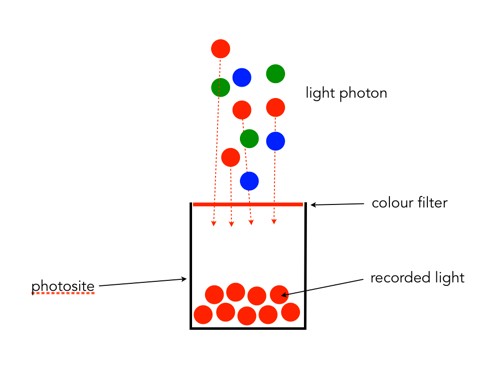
In normal mode, using a colour filter array like Bayer, each photosite acquires one particular colour, and the final colour of each pixel in an image is achieved by means of demosaicing. The basic mechanism for HRM works through sensor-shifting (or pixel-shifting) i.e. taking a series of exposures and processing the data from the photosite array to generate a single image.

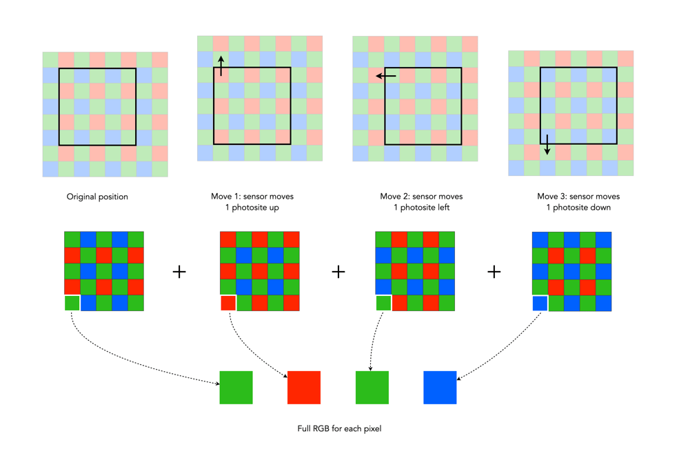
  1. An exposure is obtained with the sensor in its original position. The exposure provides the first of the RGB components for the pixel in the final image.
  2. The sensor is moved by one photosite unit in one of the four principal directions. At each original array location there is now another photosite with a different colour filter. A second exposure is made, providing the second of the components for the final pixel.
  3. Step 2 is repeated two more times, in a square movement pattern. The result is that there are four pieces of colour data for every array location: one red, one blue, and two greens.
  4. An image is generated with each RGB pixel derived from the data, the green information is derived by averaging the two green values.

No interpolation is required, and hence no demosaicing.

The basic high-resolution mode process (the arrows represent the direction the sensor shifts)

In cameras with HRM, it functions using the motors that are normally dedicated to image stabilization tasks. The motors effectively move the sensor by exactly the amount needed to shift the photosites by one whole unit. The shifting moves in such a manner that the data captured includes one Red, one Blue and two Green photosites for each pixel.

There are many benefits to this process:

  • The total amount of information is quadrupled, with each image pixel using the actual values for the colour components from the correct physical location, i.e. full RGB information, no interpolation required.
  • Quadrupling the light reaching the sensor (four exposures) should also cut the random noise in half.
  • False-colour artifacts often arising in the demosaicing process are no longer an issue.

There are also some limitations:

  • It requires a very steady scene. It doesn’t work well if the camera is on a tripod, yet there is a slight breeze, moving the leaves on a tree.
  • It can be extremely CPU-intensive to generate a HRM RAW image, and subsequently drain the battery. Some systems, like Fuji’s GFX100 uses off-camera, post-processing software to generate the RAW image.

Here are some examples of the high resolution modes offered by camera manufacturers:

  • Fujifilm – Cameras like the GFX100 (102MP) have a Pixel Shift Multi Shot mode where the camera moves the image sensor by 0.5 pixels over 16 images and composes a 400MP image (yes you read that right).
  • Olympus – Cameras like the OM-D E-M5 Mark III (20.4MP), has a High-Resolution Mode which takes 8 shots using 1 and 0.5 pixel shifts, which are merged into a 50MP image.
  • Panasonic – Cameras like the S1 (24.2MP) have a High-Resolution mode that results in 96MP images. The Panasonic S1R at 47.3MP produces 187MP images.
  • Pentax – Cameras like the K-1 II (36.4MP) use a Pixel Shift Resolution System II with a Dynamic Pixel Shift Resolution mode (for handheld shooting).
  • Sony – Cameras like the A7R IV (61MP) uses a Pixel Shift Multi Shooting mode to produce a 240MP image.

Further Reading:

From photosites to pixels (ii) – ADC

The inner workings of a camera are much more complex than most people care to know about, but everyone should have a basic understanding of how digital photographs are created.

The ADC is the Analog-to-Digital Converter. After the exposure of a picture ends, the electrons captured in each photosite are converted to a voltage. The ADC takes this analog signal as input, and classifies it into a brightness level represented by a binary number. The output from the ADC is sometimes called an ADU, or Analog-to-Digital Unit, which is a dimensionless unit of measure. The darker regions of a photographed scene will correspond to a low count of electrons, and consequently a low ADU value, while brighter regions correspond to higher ADU values.

Fig. 1: The ADC process

The value output by the ADC is limited by its resolution (or bit-depth). This is defined as the smallest incremental voltage that can be recognized by the ADC. It is usually expressed as the number of bits output by the ADC. For example a full-frame sensor with a resolution of 14 bits can convert a given analog signal to one of 214 distinct values. This means it has a tonal range of 16384 values, from 0 to 16,383 (214-1). An output value is computed based on the following formula:

ADU = (AVM / SV) × 2R

where AVM is the measured analog voltage from the photosite, SV is the system voltage, and R is the resolution of the ADC in bits. For example, for an ADC with a resolution of 8 bits, if AVM=2.7, SV=5.0, and 28, then ADU=138.

Resolution (bits)Digitizing stepsDigital values
82560..255
1010240.1023
1240960..4095
14163840..16383
16655360..65535
Dynamic ranges of ADC resolution

The process is roughly illustrated in Figure 1. using a simple 3-bit, system with 23 values, 0 to 7. Note that because discrete numbers are being used to count and sample the analog signal, a stepped function is used instead of a continuous one. The deviations the stepped line makes from the linear line at each measurement is the quantization error. The process of converting from analog to digital is of course subject to some errors.

Now it’s starting to get more complicated. There are other things involved, like gain, which is the ratio applied while converting the analog voltage signal to bits. Then there is the least significant bit, which is the smallest change in signal that can be detected.

Why camera sensors don’t have pixels

The sensor in a digital camera is equivalent to a frame of film. They both capture light and use it to generate a picture, it is just the medium which changes: film uses light sensitive particles, digital uses light sensitive diodes. These specks of light work together to form a cohesive continuous tone picture when viewed from a distance. 

One of the most confusing things about digital cameras is the concept of pixels. They are confusing because some people think they are a quantifiable entity. But here’s the thing, they aren’t. Typically a pixel, short for picture element, is a physical point in an image. It is the smallest single component of an image, and is square in shape – but it is just a unit of information, without a specific quantity, i.e. a pixel isn’t 1mm2. The interpreted size of a pixel depends largely on the device it is viewed on. The terms PPI (pixels per inch) and DPI (dots per inch) were introduced to relate the theoretical concept of a pixel to real-world resolution. PPI describes how many pixels there are in an image per inch of distance. DPI is used in printing, and varies from device to device because multiple dots are sometimes needed to create a single pixel. 

But sensors don’t really have “pixels”. They have an array of cavities, better known as “photosites”, which are photo detectors that represent the pixels. When the shutter opens, each photosite collects light photons and stores them as electrical signals. When the exposure ends, the camera then assesses the signals and quantifies them as digital values, i.e. the things we call pixels. We tend to use the term pixel interchangeably with photosite in relation to the sensor because it has a direct association with the pixels in the image the camera creates. However a photosite is physical entity on the sensor surface, whereas pixels are abstract concepts. On a sensor, the term “pixel area” is used to describe the size of the space occupied by each photosite on the sensor. For example, a Fuji X-H1 has a pixel area of 15.05 µm² (micrometres²), which is *really* tiny.

A basic photosite

NB: Sometimes you may see photosites called “sensor elements”, or sensels.